

 Home>News>Industry News>Immersion gold, HASL, OSP? A detailed explanation of the pros and cons of different PCB surface treatments for you
TRUSUN provides one-stop customized PCB solutions for global customers
Date:2026-09-04Edit:TRUSUNBrowse:5
In the production and application of PCBs, surface treatment technology not only protects the copper foil on the PCB substrate from external environmental erosion but also enhances the electrical performance and stability of the conductor surface, directly affecting the service life and application scenario adaptability of PCBs. Currently, three widely used surface treatment processes in the industry are immersion gold, spray tin, and OSP. These three processes differ in terms of process principle, performance, and applicable scenarios. Below, we will provide a detailed analysis from multiple perspectives.
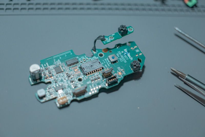
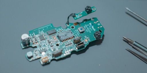
PCB Surface Finishing
1、Immersion gold: a "performance exemplar" in high-precision scenarios
Immersion gold, also known as chemical immersion gold, is a process that forms a uniform gold layer on the surface of PCB copper foil through chemical deposition. The underlying layer is usually covered with a nickel layer (nickel-gold combination), which enhances adhesion and prevents gold and copper from dissolving together.
(1)Core advantages
Excellent surface stability: Gold exhibits strong chemical inertness, making it resistant to reacting with air and moisture. It can maintain its surface cleanliness and conductivity over a long period of time. Even in complex environments such as high humidity and high temperatures, it can effectively prevent copper foil oxidation, significantly extending the storage and usage cycle of PCBs.
Uniform surface flatness: The immersion gold process results in a gold layer with extremely high thickness uniformity and low surface roughness, which can precisely meet high-precision electrical connection requirements. It is particularly suitable for scenarios where strict requirements are placed on contact resistance and signal transmission stability.
Excellent wear resistance: The hardness of the nickel-gold composite layer is higher than that of a single metal layer, making it less prone to wear under physical actions such as insertion and removal, as well as contact. This ensures connection reliability during long-term use and reduces performance degradation caused by surface wear.
(2)Main limitations
High cost threshold: As a precious metal, gold has a raw material cost that is significantly higher than other surface treatment materials. Additionally, the chemical agents used in the immersion gold process and the production control requirements are more stringent, leading to higher overall processing costs. This makes it unsuitable for cost-sensitive mid-to-low-end PCB products.
High process complexity: The immersion gold process requires strict control over parameters such as chemical solution concentration, temperature, and deposition time. Any deviation can easily lead to defects such as gold layer peeling and pinholes, thus placing high demands on the technical capabilities of the manufacturer.
2、Spray tin: the "practical choice" for cost-effective performance
Spray tinning, also known as hot air leveling, involves evenly spraying molten tin-lead alloy (or lead-free tin alloy) onto the surface of PCB copper foil, and then forming a smooth tin layer through hot air leveling. This process is widely used in mid-to-low-end PCB products due to its mature technology and moderate cost.
(1)Core advantages
Significant cost advantage: The raw material price of tin is much lower than that of gold, and the equipment investment and production process for tin spraying are relatively simple. The processing cost is only 1/3-1/2 of that for immersion gold, making it suitable for low-cost PCB needs in mass production, such as in ordinary consumer electronics, toy electronics, and other fields.
Good solderability foundation: Tin itself possesses excellent soldering properties. The tin layer formed by tin spraying provides a stable foundation for subsequent connections, and the thickness of the tin layer can be adjusted according to requirements, adapting to connection needs in different environments.
Strong process compatibility: The HASL (Hot Air Solder Leveling) process exhibits high compatibility with PCB substrate materials and copper foil thicknesses. Whether it's FR-4 substrates or paper substrates, this process can be used for surface treatment, offering high production efficiency and strong single-batch processing capability.
(2)Main limitations
Poor surface flatness: During the tin spraying process, hot air leveling can easily lead to issues such as "bridges" and depressions in the tin layer, resulting in a high surface roughness that cannot meet the requirements for surface flatness of high-precision PCBs.
Poor corrosion resistance: Tin has lower chemical stability than gold, and it is prone to oxidation when exposed to humid, acidic, or alkaline environments for extended periods. The oxide layer formed can affect electrical performance. Therefore, PCBs treated with tin spraying require additional moisture-proof packaging, and have a relatively short service life.
Lead-free transformation challenges: Traditional tin-lead alloy is used for tin spraying. Due to the harmful effects of lead on the environment, the industry has gradually shifted towards lead-free tin spraying. However, lead-free tin alloy has a higher melting point, which can easily lead to deformation of PCB substrates and requires higher adjustments to the production process.
3、OSP: An environmentally-oriented "lightweight solution"
OSP is a process that forms an ultra-thin organic protective film on the surface of PCB copper foil through chemical adsorption. This film isolates the copper foil from air contact, preventing oxidation of the copper foil while not affecting subsequent connection performance.
(1)Core advantages
Environmental protection and lightweight: OSP protective film is an organic compound that does not contain heavy metals, meeting the requirements of environmental regulations such as RoHS and REACH. Moreover, the film layer is extremely thin, which does not increase the thickness and weight of PCBs, making it suitable for ultra-thin and ultra-light PCB products.
Excellent surface flatness: The OSP film layer is formed through chemical adsorption, with uniform thickness and smooth surface, which can retain the flatness of PCB copper foil to a greater extent, even comparable to immersion gold. It is suitable for high-precision PCB scenarios, such as mobile phone motherboards, tablet PC PCBs, and other products with stringent space requirements.
Cost and process balance: The raw material cost of OSP process is lower than that of immersion gold, and the production process is simple (only requiring degreasing, micro-etching, adsorption, drying, and other steps). The processing cost is close to that of tin spraying, but the performance is better than that of tin spraying, achieving a balance of "low cost + high flatness".
(2)Main limitations
Protective film is prone to damage: The OSP film layer is extremely thin and has low hardness. During PCB transportation and storage, if it is subjected to friction, compression, or contact with oil stains, it is easy to cause damage to the film layer, exposing the copper foil and causing oxidation. Therefore, the protection requirements for packaging and handling are extremely high.
Poor temperature resistance: The high-temperature resistance of organic protective films is limited, typically only capable of withstanding short-term high temperatures of 150-200°C. If PCBs need to undergo multiple high-temperature treatments, the OSP film layer is prone to decomposition and failure, making it unsuitable for PCB products in high-temperature environments.
Short storage period: The effective protection period of OSP protective film is usually 6-12 months. After exceeding the period, the film layer will gradually age and lose its protective effect. Therefore, PCBs treated with OSP need to be processed and assembled within a short period of time and are not suitable for long-term inventory.
4、Selection suggestions for three surface treatment processes
When selecting a PCB surface treatment process, it is necessary to make a comprehensive judgment based on three core factors: application scenario, cost budget, and performance requirements
High-precision and high-reliability scenarios: If the PCB needs to meet high-frequency signal transmission and long-term stable operation (such as industrial control equipment, medical instruments, aerospace electronics), and the budget is sufficient, immersion gold plating is preferred. Its excellent stability and flatness can ensure core performance.
Low-cost, mass production scenario: If PCBs are applied to ordinary consumer electronics, low-end home appliances, and other fields with low performance requirements, and cost-effectiveness is pursued, HASL (Hasl) is the choice, which can meet basic usage requirements while controlling costs.
Ultra-thin, environmentally friendly, high-precision lightweight scenarios: If the PCB is a flexible board or ultra-thin rigid board (such as wearable devices, ultra-thin motherboards for mobile phones), and needs to meet environmental requirements, OSP is an ideal solution. Its lightweight and high flatness characteristics make it suitable for narrow spaces, while balancing cost and performance.
In summary, there is no superiority or inferiority among immersion gold, spray tin, and OSP; rather, the differences lie in their "scenario adaptability". In practical applications, it is necessary to select the appropriate surface treatment process based on the specific purpose, usage environment, and cost constraints of the PCB, in order to achieve an optimal balance between performance and cost.
Previous Article:Acceptance criteria for FPC patch processing products
Previous Article:Production process and quality control of FPC circuit boards
After the pre-treatment process of FPC electroplating, the coppe...
The design of a multi-layer PCB is different from that of a sing...
The quality of flexible printed circuit board (FPC) patch proces...
In the production and application of PCB circuit boards, surface...
As an indispensable key component in modern electronic devices, ...
 Contact TRUSUN